1
LTC3445
3445fa
Buck Regulator
?/DIV>
High Efficiency: Up to 93%
?/DIV>
600mA Output Current (V
CC1
= 3V, V
OUT
= 1.3V)
?/DIV>
Programmable Output Voltage: 0.85V to 1.55V
?/DIV>
2.5V to 5.5V Input Voltage Range
?/DIV>
1.5MHz Constant Frequency or Spread Spectrum
Option
?/DIV>
Soft-Start
LDOs
?/DIV>
Two LDO Regulators: 0.3V Dropout at 50mA
PowerPath Controller
?/DIV>
Dynamically Regulates V
CC
BATT
I
2
C
?/DIV>
Standard (100kHz) or Fast Mode (400kHz)
?/DIV>
24-Lead (4mm ?4mm) QFN Package
I
2
C Controllable
Buck Regulator with Two LDOs
in a 4mm ?4mm QFN
?/DIV>
Intels Microprocessor Supply (PXA27X)
?/DIV>
Portable Instruments
, LTC and LT are registered trademarks of Linear Technology Corporation.
The LTC
?/DIV>
3445 contains a high efficiency monolithic syn-
chronous current mode buck regulator, two LDO regula-
tors, a PowerPath
TM
controller and an I
2
C
TM
interface.
The buck regulator has a 6-bit programmable output range
of 0.85V to 1.55V. Also, the buck regulator uses either a
constant (1.5MHz) or a spread spectrum switching fre-
quency. Using the spread spectrum option allows for a
lower noise regulated output as well as low noise at the
input. In addition, the regulated output voltage slew rate is
programmable via the I
2
C interface.
The LTC3445 contains two LDO voltage regulators. The
regulator output voltages are externally resistor program-
mable. Each LDO is capable of delivering up to 50mA.
The LTC3445 contains control circuitry (PowerPath) for
automatic back-up battery selection. V
BACKUP
is typically
a coin cell.
Typical supply current during operation is only 360礎 and
drops to 27礎 in shutdown. The 2.5V to 5.5V input
voltage range makes the LTC3445 ideal for single Li-Ion
battery-powered applications. Automatic Burst Mode
?/DIV>
operation increases efficiency at light loads, further ex-
tending battery life.
Burst Mode is a registered trademark of Linear Technology Corporation.
PowerPath is a trademark of Linear Technology Corporation.
I
2
C is a trademark of Philips Electronics N.V.
Protected by U.S. Patents, including 5481178, 6580258, 6304066, 6127815, 6498466,
6611131, Spread Spectrum patent pending.
FEATURES
DESCRIPTIO
APPLICATIO S
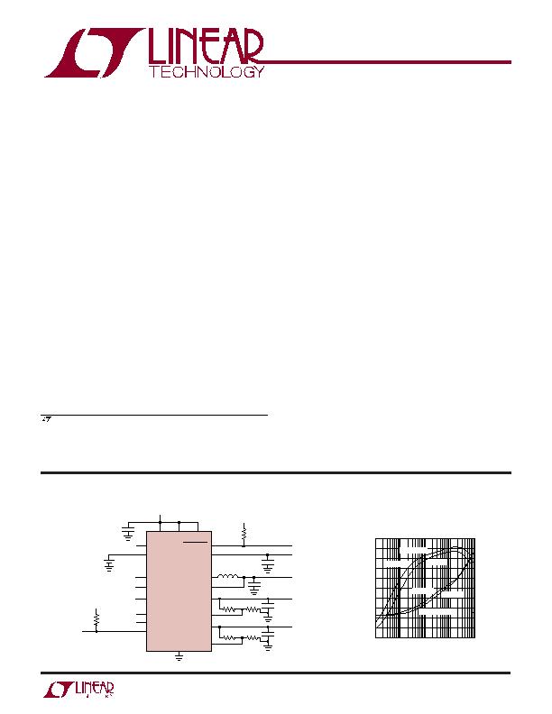
TYPICAL APPLICATIO
+
2.2礖
705k
604k
4.7礔
CER
4.7礔
CER
10礔
CER
1.3V
0.85V
TO 1.55V
3V
TYP
V
CC2
GND
LTC3445
V
CC1
nBATT_FAULT
V
CC1
BATTFAULT
4.7礔
CER
V
CC
BATT
V
TRACK
3V
COIN
CELL
V
BACKUP
LDO1
LDO1FB
LDO2
LDO2FB
SW
FB
RUN
SDA
I
2
C BUS
PWR_EN
V
CC1
OR GND
V
CC1
OR GND
SCL
ADD7
ADD6
PGOOD
V
CC
nV
CC
_FAULT
V
CC
20k
3445 TA01
503k 604k
10礔
CER
1.1V
V
BACKUP
20k
V
BACKUP
Efficiency and Power Loss
vs Load Current, V
CC1
= 3.6V
LOAD CURRENT (mA)
30
90
100
20
10
80
50
70
60
40
0.1
10 100 1000
3445 TA01b
0
1
DAC MAX
DAC MIN
DAC MIN
DAC MAX
100
1000
10
1.0
0.1
EFFICIENCY
POWER LOSS
发布紧急采购,3分钟左右您将得到回复。
相关PDF资料
LTC3446IDE#PBF
IC REG TRPL BCK/LINEAR 14-DFN
LTC3537EUD#TRPBF
IC REG DL BST/LINEAR SYNC 16-QFN
LTC3541EDD#TRPBF
IC REG DL BCK/LINEAR SYNC 10-DFN
LTC3670EDDB#TRPBF
IC REG TRPL BCK/LINEAR 12DFN
LTC3672BEDC-1#TRPBF
IC REG TRPL BCK/LINEAR 8-DFN
LTC3700EMS#TRPBF
IC REG DL BUCK/LINEAR 10MSOP
LTC4151HMS#TRPBF
IC PWR MONITOR MS 80V SD 10MSOP
LTC4210-2CS6#TRM
IC CONTROLLER HOT SWAP TSOT23-6
相关代理商/技术参数
LTC3446
制造商:LINER 制造商全称:Linear Technology 功能描述:Monolithic Buck Regulator with Dual VLDO Regulators
LTC3446EDE
制造商:LINER 制造商全称:Linear Technology 功能描述:Monolithic Buck Regulator with Dual VLDO Regulators
LTC3446EDE#PBF
功能描述:IC REG TRPL BCK/LINEAR 14-DFN RoHS:是 类别:集成电路 (IC) >> PMIC - 稳压器 - 线性 + 切换式 系列:- 标准包装:2,500 系列:- 拓扑:降压(降压)同步(3),线性(LDO)(2) 功能:任何功能 输出数:5 频率 - 开关:300kHz 电压/电流 - 输出 1:控制器 电压/电流 - 输出 2:控制器 电压/电流 - 输出 3:控制器 带 LED 驱动器:无 带监控器:无 带序列发生器:是 电源电压:5.6 V ~ 24 V 工作温度:-40°C ~ 85°C 安装类型:* 封装/外壳:* 供应商设备封装:* 包装:*
LTC3446EDE#TRPBF
功能描述:IC REG TRPL BCK/LINEAR 14-DFN RoHS:是 类别:集成电路 (IC) >> PMIC - 稳压器 - 线性 + 切换式 系列:- 标准包装:2,500 系列:- 拓扑:降压(降压)同步(3),线性(LDO)(2) 功能:任何功能 输出数:5 频率 - 开关:300kHz 电压/电流 - 输出 1:控制器 电压/电流 - 输出 2:控制器 电压/电流 - 输出 3:控制器 带 LED 驱动器:无 带监控器:无 带序列发生器:是 电源电压:5.6 V ~ 24 V 工作温度:-40°C ~ 85°C 安装类型:* 封装/外壳:* 供应商设备封装:* 包装:*
LTC3446EDE-PBF
制造商:LINER 制造商全称:Linear Technology 功能描述:Monolithic Buck Regulator with Dual VLDO Regulators
LTC3446EDE-TRPBF
制造商:LINER 制造商全称:Linear Technology 功能描述:Monolithic Buck Regulator with Dual VLDO Regulators
LTC3446IDE
制造商:LINER 制造商全称:Linear Technology 功能描述:Monolithic Buck Regulator with Dual VLDO Regulators
LTC3446IDE#PBF
功能描述:IC REG TRPL BCK/LINEAR 14-DFN RoHS:是 类别:集成电路 (IC) >> PMIC - 稳压器 - 线性 + 切换式 系列:- 标准包装:2,500 系列:- 拓扑:降压(降压)同步(3),线性(LDO)(2) 功能:任何功能 输出数:5 频率 - 开关:300kHz 电压/电流 - 输出 1:控制器 电压/电流 - 输出 2:控制器 电压/电流 - 输出 3:控制器 带 LED 驱动器:无 带监控器:无 带序列发生器:是 电源电压:5.6 V ~ 24 V 工作温度:-40°C ~ 85°C 安装类型:* 封装/外壳:* 供应商设备封装:* 包装:*